The Padding That Was Never There
Every matrix multiplication in a modern GPU starts with a small piece of housekeeping. Before the real arithmetic can begin, the input matrix has to be padded. The padding lines up its dimensions with whatever the hardware wants: a tile size, a vector width, a shared-memory bank layout, or an MMA instruction's contract. That padding is real work. It reads the original matrix, allocates a new larger buffer, writes the padding values around the edges, and stores the result back to memory. For a small matrix it is invisible. For the matrices that actually matter in modern AI and HPC workloads, it is a tax on every operation, paid in latency, in memory capacity, and in cache pollution.
A recently granted AMD patent, US12118354B2 (originally published as US20240069915A1), proposes a small, sharp answer: do not store the padding at all. A piece of hardware in front of memory lies, on behalf of the program, and synthesizes the padding values on demand. The padding was never there, and the program never has to know.
This week we are walking through that patent end to end: from the cost it is trying to remove to the small three-step decision its hardware performs on every memory access. Along the way we will see why a piece of address-level sleight of hand is interesting well beyond matrices, and where the open questions still are.
The patent at a glance
- Patent / publication number: US20240069915A1 (published application); granted as US12118354B2 on 2024-10-15
- Title: Virtually Padding Data Structures
- Assignee: Advanced Micro Devices, Inc. (AMD)
- Inventors: Meysam Taassori; Shaizeen Dilawarhusen Aga; Mohamed Assem Abd ElMohsen Ibrahim; Johnathan Robert Alsop
- Application number: US17/899,231
- Filing date: 2022-08-30
- Publication date: 2024-02-29
- Grant date: 2024-10-15
- Adjusted expiration: 2042-12-15
- Status: Active
- CPC classifications (selected): G06F 9/30 (packed data ops); G06F 12/10 (address translation); G06F 16/22 (indexing and storage structures)
- Number of claims: 20 (three independent: one method, one system, one computing device)
- Source / venue: USPTO via Google Patents, https://patents.google.com/patent/US20240069915A1/en
The hidden tax of an extra ring of zeros
To understand why this patent is interesting, it helps to picture what a modern matrix multiplication kernel actually does. GPUs and matrix engines are tiled. The hardware likes to chew on small blocks, often 16 by 16 or 32 by 32 elements, and it does the work much faster when the matrix dimensions are exact multiples of the tile size. Real matrices are rarely that polite. A 33 by 33 attention map, a 100 by 257 feature map, a 1023 by 1023 filter bank: each one needs an extra ring of values padded out to a clean multiple of the tile.
A padding function does that with brute force. It walks the original matrix element by element, copies each value into a new larger buffer, and writes the padding values into the leftover slots. The output: a real, fully materialized padded matrix sitting in physical memory.
The patent is unusually blunt about why that brute force is painful. It lists three costs, in order:
- Time cost. The original matrix has to be read, the padded version has to be written, and the writes have to retire before the real computation can start. None of that is arithmetic. It is just bookkeeping.
- Memory capacity cost. The system has to hold both matrices in memory at the same time, or at minimum allocate space for the larger padded version. For the matrices that show up in large language models, recommender systems, and scientific computing, that allocation can run straight into the limits of the device.
- Cache pollution cost. Materializing the padded matrix streams a lot of new bytes through the cache hierarchy, evicting other useful data blocks. Those evicted blocks then miss on their next access, dragging down the rest of the program.
The patent's stated goal is to remove all three of these costs at once.
Pretend padding at the address level
The core idea is to keep the padded matrix as an address-level illusion and never let it touch physical memory. AMD calls the new piece of hardware a "virtual padding unit." It sits in front of the memory management unit (MMU) and carries a small record describing two regions side by side.
The first region is the initial data structure, the non-padded matrix that actually lives in physical memory, with its location, shape, and size. The second region is the virtually padded data structure, with its own location, shape, size, and padding type: a constant value, a replicated edge value, a reflected value, or whatever else the program asked for.
Once the record is in place, the virtual padding unit does one job on every memory access that falls inside the virtual padded range. It decides, per address, which of three things should happen.
Three things can happen on any access inside the virtual padded range. If the address is outside the virtual padded region, the unit passes the address through to the MMU unchanged and the normal memory system takes over. If the address falls on a real, non-padded element of the underlying matrix, the unit translates the address into the matching address inside the original matrix and forwards it to the MMU, which performs the normal lookup and returns the actual value. If the address falls on a padding element, the unit does not issue any memory access at all. It synthesizes the padding value (constant zero, replicated edge, or reflected) and hands it directly back to the requesting processing unit.
That third case is the trick. Padding values are returned, the program gets exactly what it asked for, and no memory traffic is ever generated for the padding itself.
Three small decisions, one big saving
The hardware implementation in the patent is small enough to draw on a single piece of paper. A program issues a padding instruction that names the initial data structure and the type of padding to use. The virtual padding unit ingests that instruction and records the relationship between the initial structure and the virtual padded structure, including location, shape, size, and padding type. A system can host multiple virtual padding units, each preconfigured for a particular padding shape or type, and programs that need different paddings can pick the right one.
From that point on, every load or store issued in the virtual address range flows through the unit. The unit checks, by address range, by page table field, by dedicated bits in the issuing instruction, or by an index into a padding data table, whether the access falls into a tracked virtual padded region. The patent lists all four discrimination mechanisms and leaves the choice to the implementer. That is a good signal: the team expects different accelerators to pick whichever is most convenient for their memory subsystem.
If the access is unrelated to a virtual padded region, the unit forwards the address to the MMU. If it maps to a real element, the unit computes the matching address inside the initial matrix and forwards that. If it maps to a padding element, the unit returns the padding value directly, with no MMU walk, no cache lookup, and no DRAM access. The two caching and function-based resolution strategies the patent describes are different ways to make that third case fast. The placement diagrams (FIGS. 5, 6, and 7 in the patent) show the unit living between a processing unit and either an L1 data cache, a register file, or a load-store queue, depending on the design.
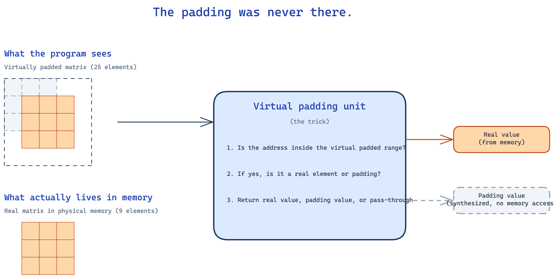
The diagram above is the entire mechanism in one picture. The program sees a padded matrix on the left. Memory only ever stores a 3 by 3 real matrix at the bottom. The virtual padding unit in the middle bridges the two with a three-step decision. The two outputs on the right are exactly what the unit hands back to the processing unit: a real value, fetched from memory, or a synthesized padding value, served without touching memory at all.
A claim family built for breadth, not narrowness
The patent's 20 claims are written for breadth, which is a useful tell about how the inventors expect the technique to land. Method, system, and device: those are the three independent claims, and each one comes with dependents that push the core idea in a slightly different direction.
The broadest method claim says: receive an address of a location in memory and output a padding value, based on the address corresponding to a padding value in the virtually padded data structure, without having stored the padding elements. The dependents add:
- applicability to virtually padded matrices specifically,
- output of the underlying address for real elements,
- pass-through for unrelated addresses,
- explicit maintenance of location, shape, and size records,
- receipt of a padding instruction that names the initial structure and padding type,
- output of a constant value,
- cache-based and function-based address resolution,
- page-table-based discrimination,
- and address-range or instruction-bit or padding-data-table discrimination.
The system claim, in turn, defines an address checking module and a module that returns a padding value when the virtual address falls in a virtual padded region, again without storing the padding. The computing device claim is the same idea expressed at the device level, with a memory management unit and a virtual padding unit that issues the address translation for real elements.
Two things are worth noticing. First, the claims are deliberately written so the data structure type is not limited to matrices. The text explicitly says the technique applies to "any of various different types of data structures, such as matrices, arrays, and so forth." Second, the padding value is not pinned to a particular scheme. Constant padding, replicated padding, and reflected padding are all explicitly in scope, which is the minimum set a useful implementation would need.
Why hardware-level padding virtualization is more interesting than it sounds
On its face, the patent looks like a micro-optimization for an obscure corner of matrix multiplication. The more you sit with it, the larger it gets.
For one thing, this is a hardware-level change, not a software trick. Compiler tricks that fold padding constants into a kernel, or JIT tricks that emit zero-fill inline, can avoid the cost in narrow cases, but they bake the padding into the code. The virtual padding unit sits below the program and below the cache hierarchy, which means a single piece of hardware can serve many different kernels and many different padding types without any code changes. For a vendor shipping a general-purpose accelerator, that is a much bigger lever.
For another, the technique composes with the existing memory system. The unit is described as cooperating with the MMU, the cache, and the register file, rather than replacing them. That makes it practical to drop into a shipping accelerator without redesigning the rest of the memory pipeline around it. The patent even notes the unit is not limited to single-level address translation. In other words, it should not break in the presence of nested page tables, huge pages, or other modern virtual memory features.
And finally, the breadth of the claims matters. AMD has not patented a clever 3 by 3 to 5 by 5 trick. It has patented a primitive: any data structure that can be expressed as a smaller real structure plus a known padding function is, in principle, a candidate for this treatment. Matrices are the first use that comes to mind, but arrays, tensors, signal-processing frames, image borders, and even some lookup tables fit the same shape. The patent is short, but the surface area of the idea is large.
What the patent does not yet tell us, and where the open questions sit
The patent is careful about its scope, and four gaps are worth naming.
It is a mechanism patent, not a performance patent. The description explains that the technique avoids the time, memory, and cache costs of materializing padding, but it does not include measured speedups, energy numbers, or area estimates. Whether the savings are large enough in real workloads to justify a piece of dedicated logic is a question left to the silicon and to the workloads that run on it.
The address-discrimination problem is not fully solved in the abstract. Determining whether a given virtual address falls on a padding element or a real element is a per-access decision, and the patent lists four alternative mechanisms, each with its own tradeoffs in latency, storage, and complexity. Real silicon will pick one or a combination, and the patent does not specify which.
The patent also leaves the question of exotic padding schemes open. Constant, replicated, and reflected padding cover the common cases, but more complex schemes (learned padding, randomized padding, content-derived padding) would need additional logic that the patent does not require. For most matrix workloads that is fine, but it does set a ceiling on what a single implementation of the unit can do.
Finally, the interactions with the rest of the memory system are sketched but not deeply explored. Huge pages, memory-mapped I/O, NUMA placement, and accelerator coherence protocols all live in the neighborhood of this unit, and the patent does not address every combination. Real deployments will have to work those out.
These caveats are not weaknesses. They are a fair map of where a small, well-targeted piece of intellectual property leaves the implementation choices. In short, what the patent claims, very clearly, is the right to build that small piece of hardware and to put it in front of a memory system. On its own, that is a useful addition to the toolbox that accelerator designers are carrying into the next generation of matrix-heavy workloads.
Sources
- US20240069915A1, "Virtually Padding Data Structures," Google Patents: https://patents.google.com/patent/US20240069915A1/en
- USPTO application US17/899,231, PatentCenter: https://patentcenter.uspto.gov/applications/17899231
- Granted patent US12118354B2 (granted 2024-10-15, expiration 2042-12-15), as listed in the Google Patents legal events for the same family
- Espacenet publication record: https://worldwide.espacenet.com/publicationDetails/biblio?CC=US&NR=2024069915A1&KC=A1&FT=D
- CPC classifications as assigned on the Google Patents record: G06F 9/30, G06F 12/10, G06F 16/22, and related G06F 12/02, G06F 12/08, G06F 9/30003, G06F 9/30007, G06F 9/30036, G06F 16/20, G06F 16/2228, G06F 16/2237 classifications